Last updated: Nov 10th 2021
Security Closure
Introduction, Contest Outline
CAD tools traditionally optimize for PPA. However, considering that various and serious threats are emerging, future CAD flows should also incorporate techniques for secure IC design.
This contest is focused on security closure of physical layouts, that is, on hardening the physical layouts at design time against various threats that are executed post-design time. This topic is important for multiple reasons. First, many threats, like Trojan insertion or side-channel attacks, are directly targeting vulnerabilities of the physical layouts. Second, threats that are not mitigated during design-time are almost impossible to fix later on; ICs are unlike patchable software. Third, even if efforts are taken toward secure IC design at higher abstraction layers, like high-level synthesis or logic synthesis, such efforts may be undermined by, e.g., PPA optimization, thus becoming futile without dedicated support for security closure at layout level.
Secure-by-design and security closure are two related, emerging paradigms for CAD tools. Secure-by-design means to support 1) top-down propagation and translation of security requirements and specifications and 2) bottom-up verification and validation of defenses against attacker’s technical capabilities and limitations. Security closure is the specific paradigm for the physical design, conceptually similar to other sign-off stages like timing closure but focused on security. Means for security closure will be based on ECO placement, routing, etc., as needed. A secure-by-design CAD flow with integrated means for security closure is outlined next.
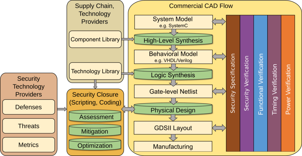
The objective of this contest is the following: implement measures for security closure to proactively harden layouts against post-design Trojan insertion at gate level and against post-design electro-optical or contact-based probing, fault injection attacks targeting at the frontside. More details on those threats and the implications for security closure are discussed below, in the section on Hardware Security.
To achieve this objective, participants would want to, e.g., control placement and routing in such a way that insertion of Trojan components (trigger and payload) as well as probing and fault injection on particular devices or wires becomes difficult. The former is supported by, e.g., control of placement sites and routing resources, whereas the latter is supported by, e.g., other metal segments obstructing the line of sight/attack vector.
To enable a fair contest, we have to restrict the scope of defense efforts to the physical design stages. Thus, we do not allow to, e.g., introduce dedicated sensor circuitry. Please also see the Evaluation page for more details on constraints as well as for some guidance for permissible defense efforts.
As indicated, efforts are to be focused on physical design stages, implying that measures for security closure against these different threats can be streamlined. At the same time, the impact of the measures on design quality must be considered as well. Given that there are various, quite different metrics to be considered for design quality and security closure at once, some machine learning-based guidance can be promising here. In any case, there is no single, right or wrong approach toward that end — it is up to your creativity and skills to come up with the best defense solutions.
References
-
- J. Knechtel, J. Gopinath, J. Bhandari, M. Ashraf, H. Amrouch, S. Borkar, S.-K. Lim, O. Sinanoglu, and R. Karri, “Security closure of physical layouts,” in Proc. IEEE/ACM Int. Conf. Comput.-Aided Des. (ICCAD), 2021
PDF - J. Knechtel, E. B. Kavun, F. Regazzoni, A. Heuser, A. Chattopadhyay, D. Mukhopadhyay, S. Dey, Y. Fei, Y. Belenky, I. Levi, T. Güneysu, P. Schaumont, and I. Polian, “Towards secure composition of integrated circuits and electronic systems: On the role of EDA,” in Proc. EDAA/ACM/IEEE Des. Autom. Test Eur. (DATE), pp. 508-513, 2020 (DOI: 10.23919/DATE48585.2020.9116483)
PDF
- J. Knechtel, J. Gopinath, J. Bhandari, M. Ashraf, H. Amrouch, S. Borkar, S.-K. Lim, O. Sinanoglu, and R. Karri, “Security closure of physical layouts,” in Proc. IEEE/ACM Int. Conf. Comput.-Aided Des. (ICCAD), 2021
Hardware Security
Introduction, Contest Outline
There are various challenges or rather threats to consider when we talk about hardware security. An overview on threats linked to the different stages of the IC supply-chain and life-cycle is shown next.
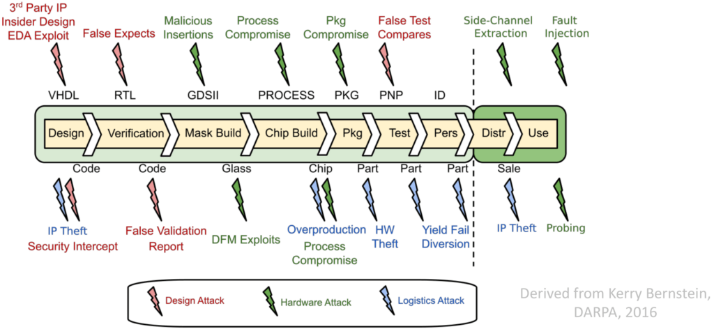
The main threats of current interest to the community are 1) Trojans, 2) side-channel attacks, 3) fault-injection attacks, 4) probing attacks, and 5) IP piracy. Typically, each kind of threat is further divided/categorized; for example, there is direct physical fault injection, e.g., using laser light, voltage glitches, etc., versus indirect fault injection, e.g., repetitive writing to physical memory locations (also known as “Rowhammer” attack). Some threats share a similar physical attack vector, like laser fault injection and laser-assisted optical probing.
The threats relevant for this contest are Trojan insertion at the gate level as well as probing, fault injection targeting the frontside (metal layers). More details on those threats and aspects relevant for this contest are discussed next.
Hardware Trojans
Trojans are malicious hardware modifications. The notion of Trojans is diverse, covering malicious hardware modifications that are: (i) targeting at the system level, RTL, gate/transistor level, and/or the physical level; (ii) seeking to leak information from an IC, reduce the IC’s performance, or disrupt an IC’s working altogether; (iii) are always on, triggered internally, or triggered externally. Most Trojans comprise a trigger and a payload; the trigger activates the payload on attack conditions, and the payload serves to perform the actual attack.
Since IC supply-chains are nowadays largely outsourced, adversaries at various entities could introduce such Trojans, e.g., through untrustworthy third-party IP, by adversarial designers, during mask generation or manufacturing, or even during distribution or deployment of ICs.
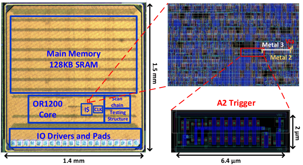
For this contest, we focus on Trojans that are inserted at the gate level (post-design, i.e., during mask generation or manufacturing). An example of such a Trojan is shown next. More specifically, illustrated is the die snapshot of an OR1200 processor with the so-called A2 Trojan embedded, with the zoom-in highlighting the additional logic inserted for the Trojan trigger. The payload of the A2 Trojan, maliciously setting the privilege mode of the OR1200 processor, is not highlighted separately, only the additional routing toward the privilege-mode register is indicated by white/yellow wiring (labelled Metal3/2).
For those interested in more details for this particular Trojan, see Yang et al., listed in the references below; however, such details are not required to tackle the contest.
The related task for this contest is to proactively harden the layouts against post-design Trojan insertion. This means to, e.g., control placement and routing in such a way that insertion of Trojan components (trigger and payload) becomes difficult, but also considering impact on design quality of such measures at the same time.
As indicated, there is no single, right or wrong approach toward that end — it is up to your creativity and skills to come up with the best defense solutions. However, to enable a fair contest, we have to restrict the scope of defense efforts to the physical design stages. Thus, we do not allow to, e.g., introduce dedicated sensor circuitry. Please also see the Evaluation page for more details on constraints as well as for some guidance for permissible defense efforts.
Probing, Fault Injection Targeting the Frontside
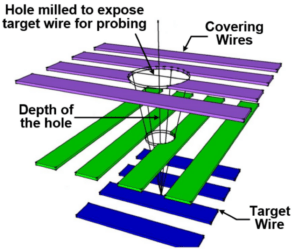
Probing attacks extract data from cells or wires by probing the layout at the frontside (metal layers) or the backside (substrate). Such attacks are enabled by different means, like contact-based micro-probing, electro-magnetic field probing, or electro-optical device probing. These various means leverage different physical vectors, like electro-magnetic field emissions, electrical charges, photon injection and emission, etc. Probing attacks have their roots in failure analysis techniques, hence also apply for advanced nodes. Some attacks like micro-probing require line of sight and direct access to the cell/wire of interest; thus, such attacks are often complemented by techniques like focused ion beam milling.
Fault-injection attacks induce faults to aid deducing sensitive information. Therefore, fault injection can support and advance side-channels attacks or other analytical attacks. Fault-injection attacks cover direct fault injection, e.g., using laser light or electromagnetic waves, as well as indirect fault injection, e.g., by repetitive writing to particular memory locations or by deliberate misuse of dynamic voltage and frequency scaling (DVFS) features.
For this contest, we focus on probing and fault injection targeting the frontside. We understand that attacks targeting at the backside are more capable, relevant, and practical. However, defending the backside requires dedicated circuitry or technology support, e.g., current sensors or backside metal layers, whereas defending the frontside can be realized via physical design efforts. Please also see the Evaluation page for more details on constraints as well as for some guidance for permissible defense efforts.
An illustrative example for such a frontside attack is given next. Here, milling through metal layers (e.g., using focused ion beam) is done to enable subsequent contact-based micro-probing. Note the conical shape of the milling intrusion, and also note the challenge for an attacker to avoid cutting wires critical to the operation of the IC.
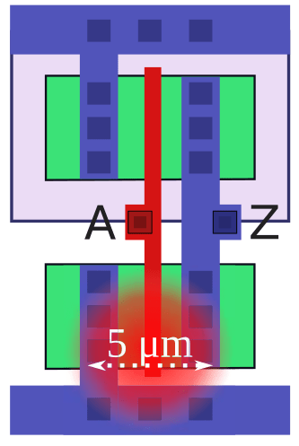
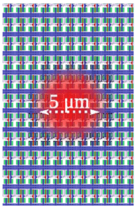
Consider another illustrative example. Here, laser light is injected into the active device layer for different technology nodes, hence the spatial scope of the related fault injection differs: for older nodes (250nm, shown top), individual transistors can be targeted at, whereas for newer nodes (28nm, shown below), multiple adjacent cells will be targeted at once. For better visibility, metal layers are not shown here.
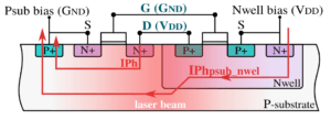
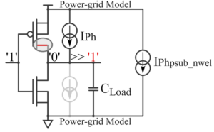
Note that the impact of laser light on transistors can be modeled as transient photocurrents, possibly affecting multiple/different PN junctions, thereby possibly affecting the switching of transistors as well as the IR drop of the related cell. Illustrated next are the photocurrent paths (left) and the impact on the switching operation (right) for an inverter.
For those interested in more details on laser fault injection, see De Castro et al. or Viera et al., both listed in the references below; however, such details are not required to tackle the contest.
Note that electro-optical probing has a similar physical attack vector; laser light is used for stimulation of active devices to assist reading out their data at runtime. More generally, electro-optical or contact-based probing and fault injection targeting at the frontside share the same attack principle, namely to “sneak through” metal layers down to active devices or wires of interest.
The related task for this contest is to proactively harden the layouts against post-design probing and fault injection attacks targeting the frontside. This means, e.g., to control placement and routing in such a way that probing/fault injection on particular devices or wires becomes difficult, namely by nature of some (other) metal segments obstructing the line of sight required for such attacks. At the same time, the impact on design quality of such defense measures must be considered.
As indicated, there is no single, right or wrong approach toward that end — it is up to your creativity and skills to come up with the best defense solutions. However, to enable a fair contest, we have to restrict the scope of defense efforts to the physical design stages. Thus, we do not allow to, e.g., introduce dedicated sensor circuitry. Please also see the Evaluation page for more details on constraints as well as for some guidance for permissible defense efforts.
References
-
- J. Knechtel, “Hardware security for and beyond CMOS technology,” in Proc. ACM Int. Symp. Phys. Des. (ISPD), pp. 115-126, 2021 (DOI: 10.1145/3439706.3446902)
PDF - Rangarajan N., Patnaik S., Knechtel J., Rakheja S., Sinanoglu O. (2021) Introduction. In: The Next Era in Hardware Security. Springer.
DOI: 10.1007/978-3-030-85792-9_1 - W. Hu, C. -H. Chang, A. Sengupta, S. Bhunia, R. Kastner and H. Li, “An Overview of Hardware Security and Trust: Threats, Countermeasures, and Design Tools,” in IEEE Transactions on Computer-Aided Design of Integrated Circuits and Systems, vol. 40, no. 6, pp. 1010-1038, June 2021
DOI: 10.1109/TCAD.2020.3047976 - K. Xiao et al., “Hardware trojans: Lessons learned after one decade of
research,” Trans. Des. Autom. Elec. Sys., vol. 22, no. 1, 2016
DOI: 10.1145/2906147 - Stephan De Castro, Jean-Max Dutertre, Bruno Rouzeyre, Giorgio Di Natale, and Marie-Lise Flottes. 2016. Frontside Versus Backside Laser Injection: A Comparative Study. J. Emerg. Technol. Comput. Syst. 13, 1, Article 7 (December 2016)
DOI: 10.1145/2845999 - K. Yang, M. Hicks, Q. Dong, T. Austin and D. Sylvester, “A2: Analog Malicious Hardware,” 2016 IEEE Symposium on Security and Privacy (SP), 2016, pp. 18-37
DOI: 10.1109/SP.2016.10 - R. A. C. Viera, P. Maurine, J. -M. Dutertre and R. Possamai Bastos, “Simulation and Experimental Demonstration of the Importance of IR-Drops During Laser Fault Injection,” in IEEE Transactions on Computer-Aided Design of Integrated Circuits and Systems, vol. 39, no. 6, pp. 1231-1244, June 2020
DOI: 10.1109/TCAD.2019.2928972 - H. Wang, D. Forte, M. M. Tehranipoor and Q. Shi, “Probing Attacks on Integrated Circuits: Challenges and Research Opportunities,” in IEEE Design & Test, vol. 34, no. 5, pp. 63-71, Oct. 2017
DOI: 10.1109/MDAT.2017.2729398
- J. Knechtel, “Hardware security for and beyond CMOS technology,” in Proc. ACM Int. Symp. Phys. Des. (ISPD), pp. 115-126, 2021 (DOI: 10.1145/3439706.3446902)